Co.,Ltd.")
Co.,Ltd.")
 CN
CN
 EN
EN

Product Overview
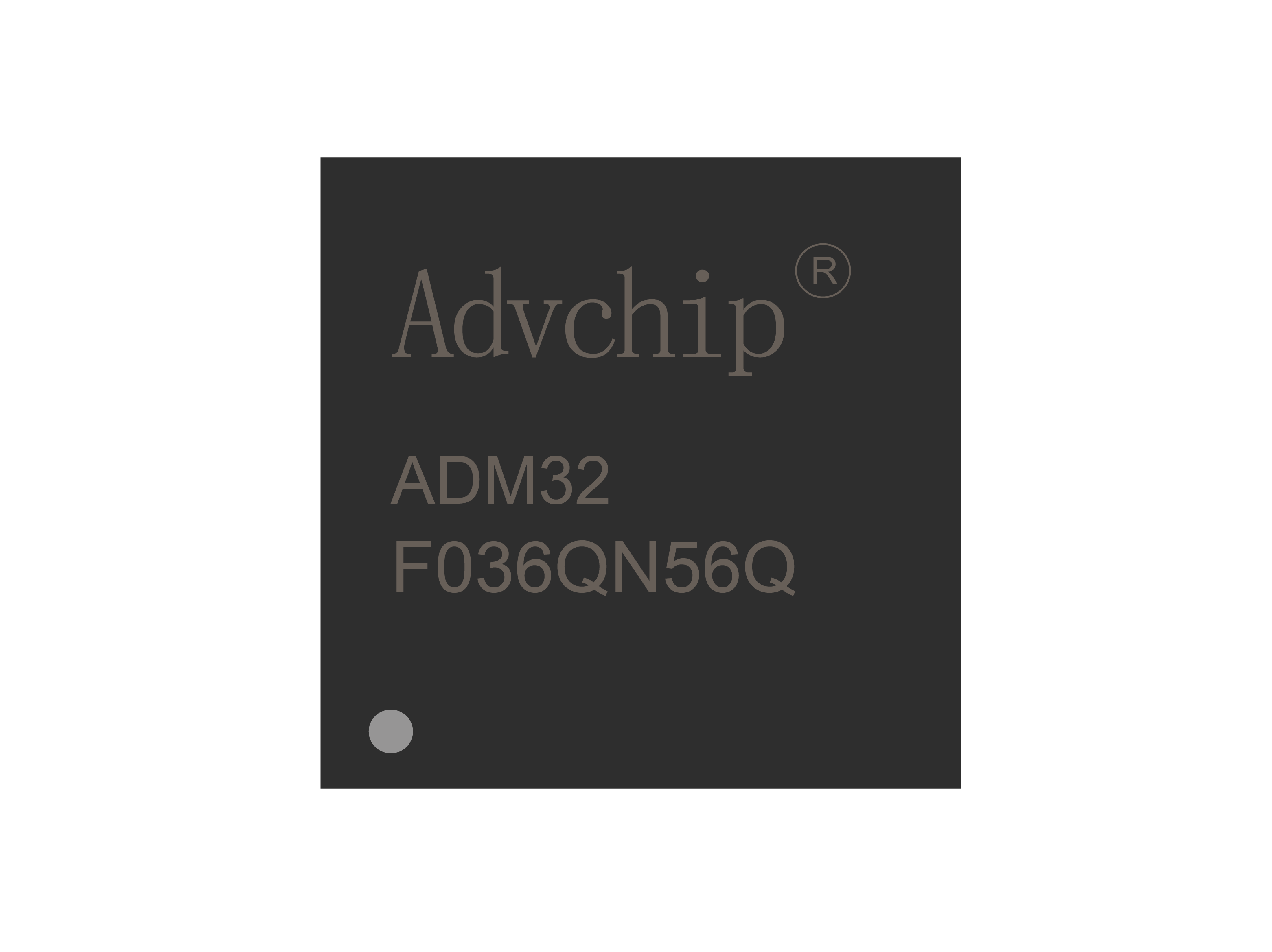
ADM32F036Q
ADM32F036Q is a high-performance SoC designed for automotive applications, with a main frequency of 100MHz and a built-in CLA operation accelerator. It integrates operational amplifiers, comparators, ADCs, (HR) PWM controllers, as well as pre drivers and LDOs for communication peripherals such as SCI, SPI, IIC, CAN/CAN-FD, LIN, etc. It is directly powered by 12V and has high integration; AEC-Q100 certification
Datasheet →Automotive Standard
Product Features
● Single source power supply
-4.5~60V
- Integrated LDO
- Integrated POR and BOR circuits (LDO12V, IO 5V, core 1.2V, analog 3.0V)
● High performance 32-bit fixed-point DSP core
-100MHz
-16 × 16, 32 × 32 MAC Operation
-16 × 16 Dual MAC Operation
- Harvard Bus Structure
- Fast Interrupt Response and Processing
● Programmable Control Law Acceleration Unit (CLA)
-32-bit Floating Point Acceleration Unit
- Acceleration Code and CPU Parallel code execution
● on-chip memory resources
-18K x 16 bit SARAM
-13 channels, with temperature sensor channels
- input range 0~3V, internal reference
● operational amplifier
-1 OP, can be used for bus current detection amplification
-2 PGAs, can be used for phase current detection amplification
10} ● Integrated three-phase high and low side half bridge drive circuit
- Six channel NMOSPre Driver
- Gate drive circuit high side floating voltage reaches 60V
- Drive capability IO+/IO -:+1.8A/1.5A
● Voltage comparator
-3 External or built-in 8-bit DAC voltage reference for voltage comparator, output associated with TZ, supporting periodic waveform protection
● Enhanced control peripherals
-3 32-bit timing/counters
-5 16 bit timing/counters
-2 PWM outputs (1 supporting HRPWM)
● Serial communication peripherals
- CAN, SPI, SCI, LIN, IIC
-1-channel CANFD
● IO
- Quartz crystal oscillator/external input mode
- PLL multiplication coefficient 1x~12x
● Supports WDT
● Support JTAG online simulation
- analysis and breakpoint functions
- hardware based real-time debugging
● QFN56 package
● Temperature range -40 ℃~+125 ℃
● AEC-Q100 certification
-4.5~60V
- Integrated LDO
- Integrated POR and BOR circuits (LDO12V, IO 5V, core 1.2V, analog 3.0V)
● High performance 32-bit fixed-point DSP core
-100MHz
-16 × 16, 32 × 32 MAC Operation
-16 × 16 Dual MAC Operation
- Harvard Bus Structure
- Fast Interrupt Response and Processing
● Programmable Control Law Acceleration Unit (CLA)
-32-bit Floating Point Acceleration Unit
- Acceleration Code and CPU Parallel code execution
● on-chip memory resources
-18K x 16 bit SARAM
-64K x 16 bit Fl ash
-8K x 16 bit BootROM● 128 bit key
● ADC
-12 bit SAR, conversion rate 4MSPS-13 channels, with temperature sensor channels
- input range 0~3V, internal reference
● operational amplifier
-1 OP, can be used for bus current detection amplification
-2 PGAs, can be used for phase current detection amplification
10} ● Integrated three-phase high and low side half bridge drive circuit
- Six channel NMOSPre Driver
- Gate drive circuit high side floating voltage reaches 60V
- Drive capability IO+/IO -:+1.8A/1.5A
● Voltage comparator
-3 External or built-in 8-bit DAC voltage reference for voltage comparator, output associated with TZ, supporting periodic waveform protection
● Enhanced control peripherals
-3 32-bit timing/counters
-5 16 bit timing/counters
-2 PWM outputs (1 supporting HRPWM)
-1 high-precision capture unit
tag10} ● Interrupts
-53 interrupts set by PIE● Serial communication peripherals
- CAN, SPI, SCI, LIN, IIC
-1-channel CANFD
● IO
-16 universal IOs
● Clock
-10M on-chip oscillator- Quartz crystal oscillator/external input mode
- PLL multiplication coefficient 1x~12x
● Supports WDT
● Support JTAG online simulation
- analysis and breakpoint functions
- hardware based real-time debugging
● QFN56 package
● Temperature range -40 ℃~+125 ℃
● AEC-Q100 certification


Co.,Ltd.")