Co.,Ltd.")
Co.,Ltd.")
 CN
CN
 EN
EN

Product Overview
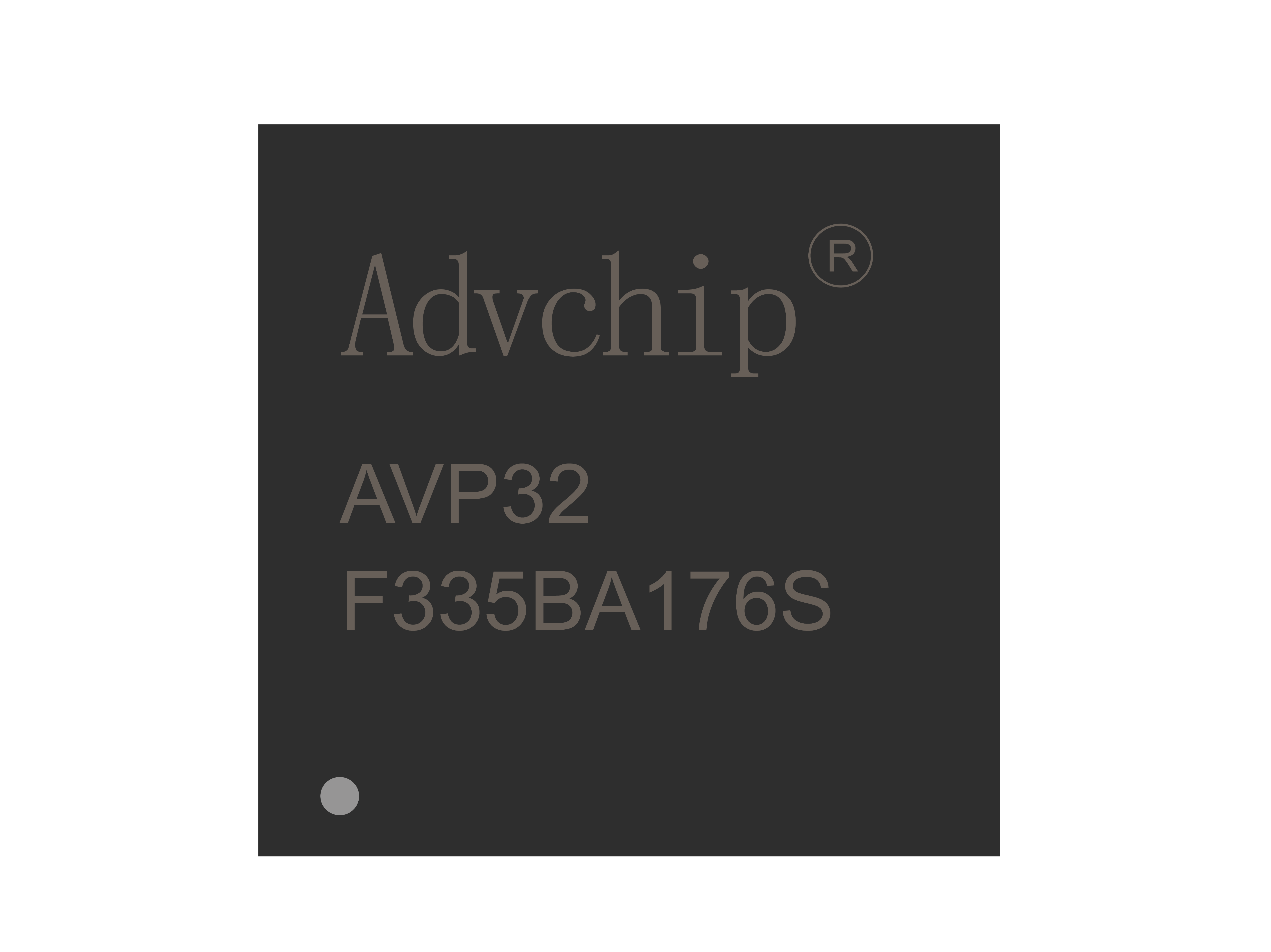
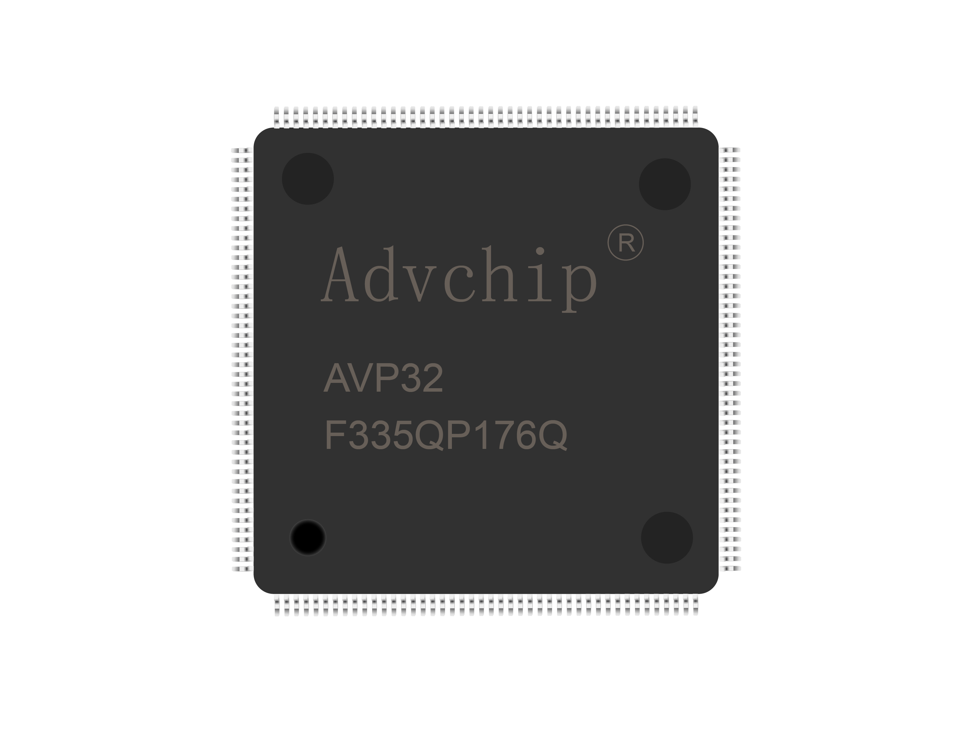
AVP32F335
AVP32F335 is a 32-bit fixed-point and floating-point digital signal processor that supports a clock frequency of 150 MHz and has powerful computing capabilities. It integrates multiple types of memory, enhanced peripherals, communication interface peripherals, and analog peripherals internally, supports QFP176 and BGA176 packaging, and has passed AEC-Q100 automotive certification. It can be widely used in industrial motor drives, photovoltaic inverters and digital power supplies, electric vehicles and transportation, motor control, as well as sensing and signal processing fields.
Datasheet →industry Automotive Standard
Product Features
● High performance static CMOS technology
- up to 150MHz (6.67ns cycle time)
-1.8V to 1.65V core, 3.3V I/O design
● High performance 32-bit CPU
- I EEE-754 single precision floating-point unit (FPU)
-16 x 16 and 32 x 32 medium access control (MAC) operations tag13 -16 x 16 dual MACs
- Harvard bus architecture
- Fast interrupt response and processing
- Unified memory programming model
- Code (using C/C++and assembly language)
● 6-channel DMA processor (for ADC, McBSP, ePWM, X I NFT, and others) SARAM)
● 16 bit or 32-bit external interface (X I NFT)
- address range exceeding 2M × 16
● on-chip memory
-256K × 16 flash memory, 34K × 16 SARAM
-1K x 16 one-time programmable (OTP) ROM
● Boot ROM (8K X 16)
- Supports software boot mode (via ) SCI , SPI, CAN, I2C, McBSP, XINTF, and parallel I/O)
- Standard digital table
● Clock and system control
- Supports dynamic phase-locked loop (PLL) ratio changes
- On chip oscillator
- Watchdog timer module
● GPO0 to GPO63 pins can be connected to one of eight external cores for interrupt.
● Peripheral Interrupt Extension (PIE) block that supports all 58 peripheral interrupts
● 128 bit secure key/lock
- protects flash/OTP/RAM modules
- prevents firmware reverse engineering
Low power mode and power-saving mode
- supports I DLE (idle), STANDBY (standby) HALT (pause) mode
● Byte order: small end order
● ESD level (HBM): 2000V
● MSL humidity sensitivity level: 3
● Enhanced control peripheral
- up to 18 pulse width modulation (PWM) outputs
- Up to 6 high-resolution pulse width modulators (HRPWMs) supporting 150ps micro boundary localization (MEP) resolution outputs
- Up to 6 event capture inputs
- Up to two orthogonal encoder interfaces
-8 32-bit timers (6 eCAPs, 2 eQEPs)
-9 32-bit timers (6 ePWMs, 3 XINTCRs)
● Three 32-bit timers CPU timers
● Serial port peripherals
-2 Controller Area Network (CAN) modules
-3 SCI (UART) modules
-2 McBSP modules (configurable as SPI)
-1 SPI module
-1 Internal Integrated Circuit (I2C) bus
12 bit analog-to-digital converter (ADC), 16 channels
-12 bits -267ns conversion rate
-2 x 8-channel input multiplexer
- two sample and hold
- sequential/concurrent conversion
- internal or external reference
● Up to 88 individually programmable multiplexed general-purpose input/output (GPIO) pins with input filtering capabilities
● JTAG boundary scan support
● Simulation features
- Analysis and breakpoint functionality
- Hardware real-time debugging
● Development support includes
- ANSI C/C++compiler/assembly Language/Connector
- Compiler
- Digital Motor Control and Digital Power Software Library
Product model
- AVP32F335QP176S
- AVP32F335QP176S1
- AVP32F335BA176S

Co.,Ltd.")