Co.,Ltd.")
Co.,Ltd.")
 CN
CN
 EN
EN

Product Overview
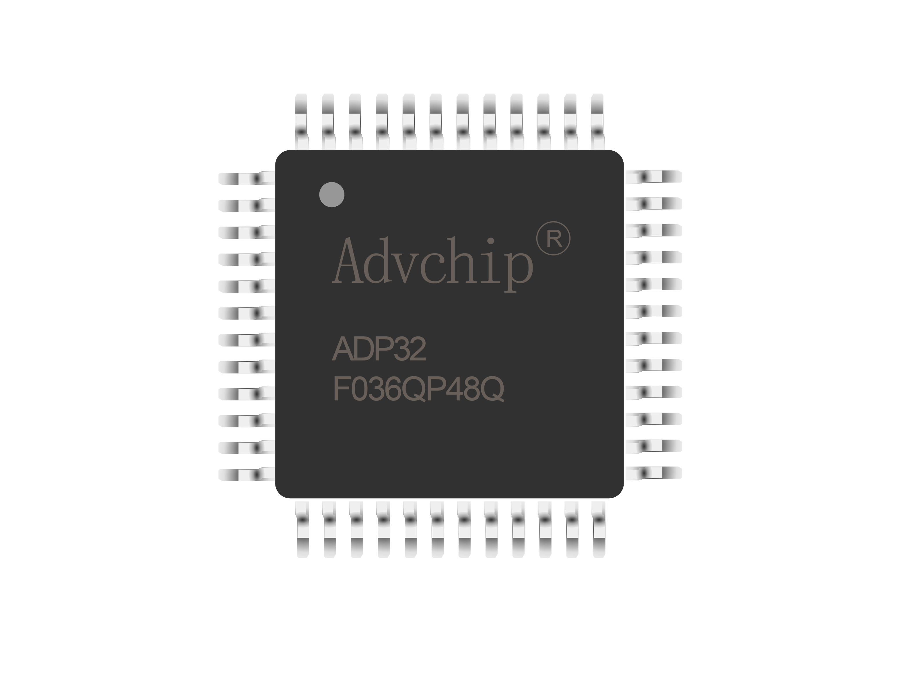
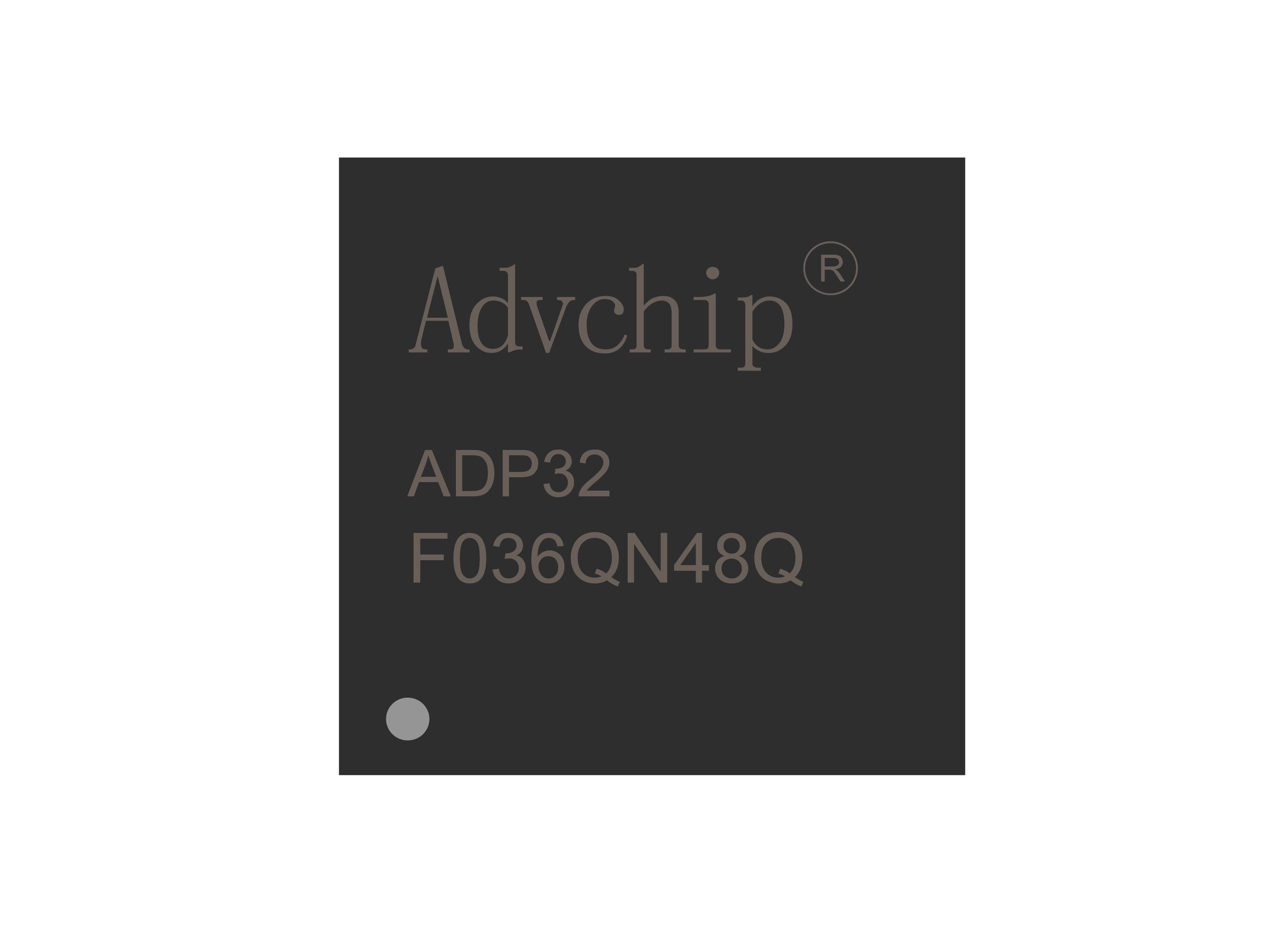
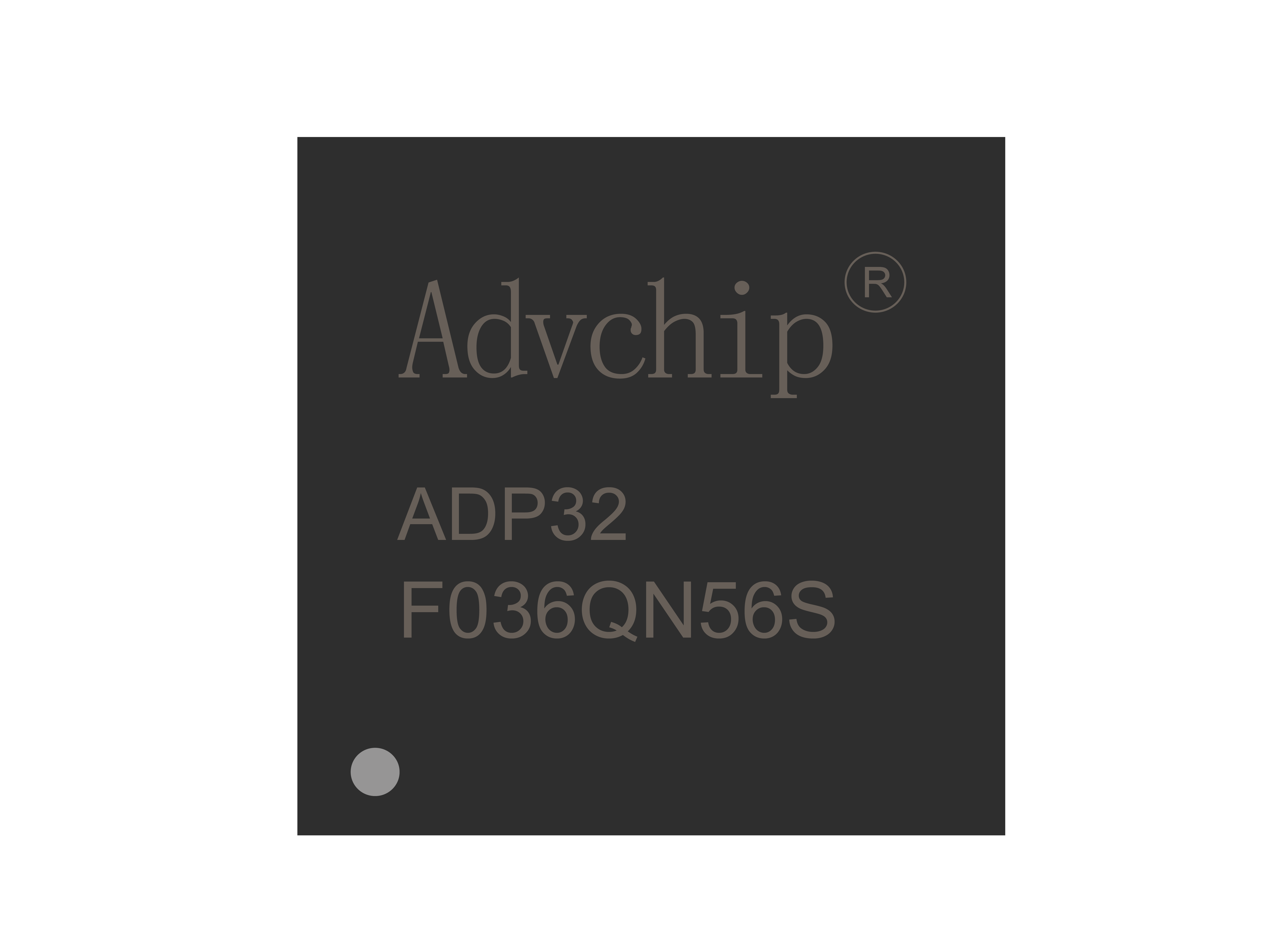
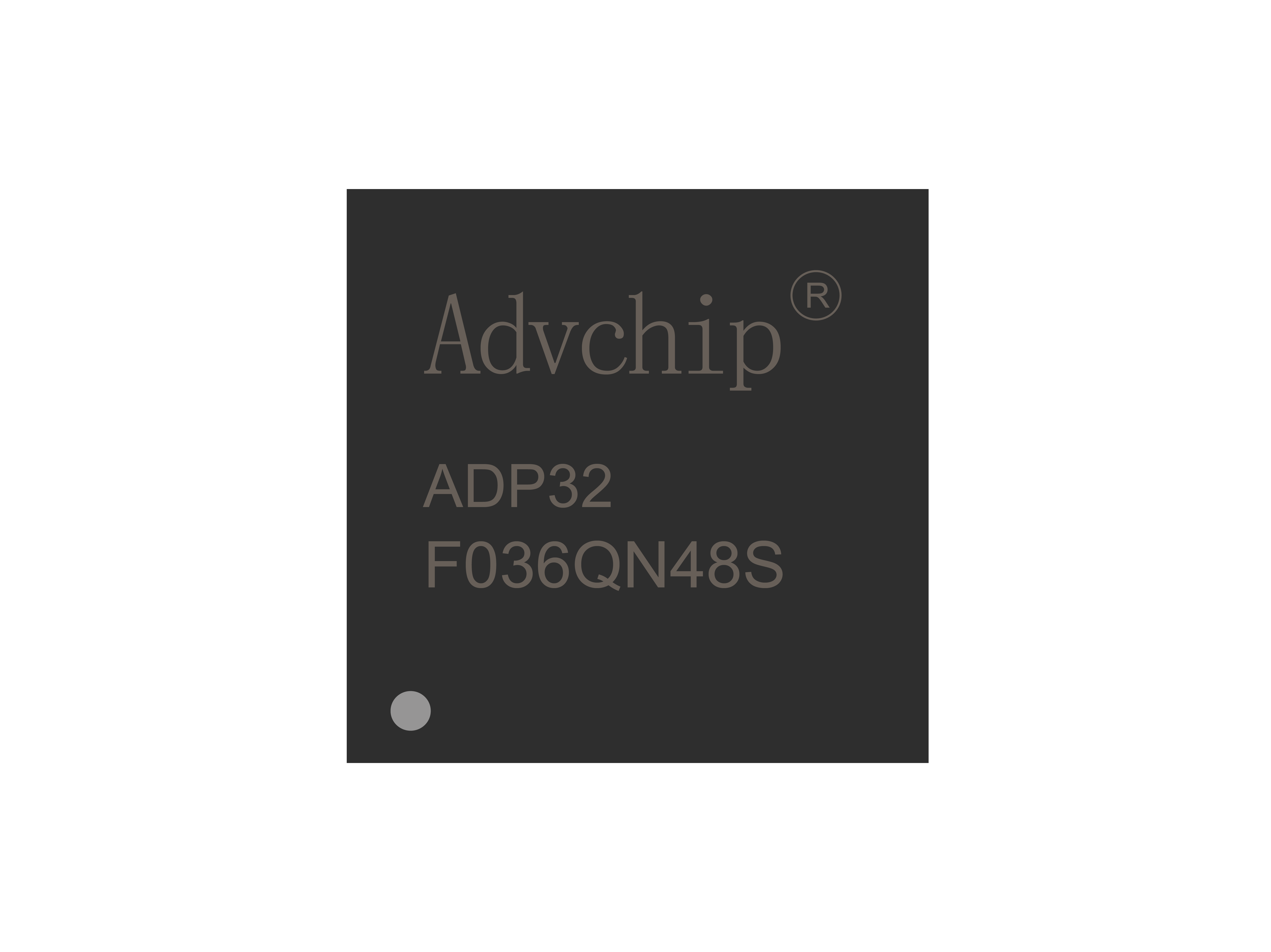
ADP32F036
ADP32F036 is a high-performance 32-bit fixed-point DSP with a clock frequency of up to 100MHz, built-in CLA operation accelerator, integrated operational amplifier, comparator, ADC, (HR) PWM controller, and communication peripherals such as SCI, SPI, IIC, CAN \ CAN-FD, LIN, etc.
Datasheet →工业 车规
Product Features
● High performance 32-bit fixed-point DSP core
- Main frequency 100MHz
-16 x 16 and 32 x 32 multiply accumulate MAC operations
-16 x 16 dual MAC operations
- Harvard bus architecture
- Fast interrupt response and processing
● Programmable Control Law Acceleration Unit (CLA)
-32-bit floating-point arithmetic accelerator
- Acceleration code runs parallel to CPU code
● Single power supply
- IO 3.3~5V, kernel 1.2V
- Integrated POR and BOR circuits
● on-chip memory resources
-18K x 16 bit SARAM (ECC or parity protection)
-64K x 16 bit Flash
-8K x 16 bit BootROM
-1K x 16 bit OTP
● diagnostic features
- memory boot self-test
● 128 bit security key
● ADC
-12 bit SAR, conversion rate 4MSPS
-15 channels, including 1 temperature sensor channel
- input range 0~3V, internal reference
● Operational amplifier
-1 OP, Can be used for bus current detection amplification
-3 PGAs, can be used for phase current detection amplification
● Voltage comparator
-3 voltage comparators
- External or built-in 8-bit DAC voltage reference
- Output associated TZ, supports periodic wave sealing protection
● Enhanced control peripheral
-3 32-bit timer/counters
-5 16 bit timer/counters
-10 PWM outputs (5 supporting HRPWM)
-2 capture units (CAP1/HRCAP1)
● Interrupts
-54 by PIE Interrupts set
● Serial communication peripherals
- CAN, SPI, SCI, LIN, IIC
-1-channel CANFD
● IO
-27 universal IO
● Clock
-10M on-chip oscillator
- Quartz crystal oscillator/external input mode
- PLL multiplication coefficient 1x~12x
● Supports WDT
● Code security for on-chip flash memory/SARAM/OTP blocks
● Supports JTAG online simulation
- Analysis and breakpoint function
- Hardware based real-time debugging
● LQFP48 packaging
● QFN48 packaging
● QFN56 packaging
● Temperature range Q : - 40 ℃~+125 ℃ (certified by AEC-Q100)

Co.,Ltd.")