Co.,Ltd.")
Co.,Ltd.")
 CN
CN
 EN
EN

ADP32F1x
ADP32F1X is a 32-bit fixed-point digital signal processor with a main frequency of 150MHz. It integrates a 12 bit ADC, PWM controller, sensor acquisition, and various communication peripherals. It can be extended by XINTF and supports connection with FPGA.
Datasheet →工业
• Adopting high-performance CMOS technology
- main frequency 150MHz (period 6.67ns)
- low-power design (core 1.8V, I/O voltage 3.3V)
- integrated on-chip 1.8V linear voltage regulator (LDO)
• Supporting JTAG online simulation
• High performance 32-bit CPU
- single cycle 32-bit x32 bit multiply accumulate add (MAC) operation
- single cycle 2 16 bit x16 bit multiply accumulate (MAC) operation
- Harvard bus architecture
9} - Atomic operations- Fast interrupt response and processing
- Unified register programming mode
-4M linear program/data address
- Programmable with C/C++and assembly language rates
• on-chip memory resources
- Flash memory: 128K x 16 bit flash memory
( 4 8Kx16 bits and 6 16Kx16 bit sectors)
- ROM : 128K X 16 bit ROM (note: C version, needs to be customized by the customer) -1K x 16 one-time programmable (OTP) ROM
- L0 and L1: 2 blocks of 4Kx16 bit independent addressing SARAM - H0: 1 block of 8K x 16 bit SARAM tag17}
- M0 and M1: 2 blocks of 1Kx16 bit independent addressing SARAM
• Guidance ROM (4K X 16
- supports software boot mode
- comes with a standard arithmetic table
• external storage extension interface
- expandable space of over 1M x 16 bits
16} - Programmable waiting state
- Programmable read/write timing -3 independent chip selection signals
• Clock and system control
- - Supports dynamic phase-locked loop (PLL) Frequency division coefficient adjustment
- On-chip oscillator
- watchdog timer
• Three external interrupt interfaces
• Peripheral interrupt extension block supporting 45 peripheral interrupts (P } I E )
• Three 32-bit CPU timers
• 128 bit secure key/lock
- protects flash memory/ROM/OTP and L0/L1 SARAM
- prevents firmware reverse cracking
• Motor control peripheral (PWM generation circuit)
- Event Manager 1 (EM1), Event Manager 2 (EM2)
- Each includes: 2 16 bit timers, 3 numerical comparators, 3 capture units, and 1 orthogonal encoding circuit.
• Serial Port Peripheral
- Serial Peripheral Interface (SPI)
-2 Serial Communication Interfaces (SCI), compatible with Universal Asynchronous Receiver/Transmitter (UART) standard
- Enhanced Controller Area Network (eCAN) controller, integrated on-chip eCAN driver
- Multi Channel Buffer Serial Port (McBSP)
• 12 bit 16 channel analog-to-digital converter (ADC)
-2 x 8-channel input multiplexers
- Two sample and hold circuits
- Single/synchronous conversion
- Fast conversion rate: 80ns/12.5MSPS
• 56 General I/O (GPIO) pins
• Advanced simulation functions
- analysis and breakpoint functions
- - Real time debugging based on hardware tag17}
development tool
- C/C++ compiler / assembly language / connector
- JTAG emulator tag17}
• Low power mode and power-saving mode
- Supports IDLE (idle), STANDBY (standby ), HALT (Pause) Mode
- Disabled independent peripheral clock
• Powerful electrostatic discharge (ESD) protection capability
- ESD human mode (HBM):+4000V/-4000V - ESD machine mode (MM):+400V/-400V
- Latch up trigger current: 400mA
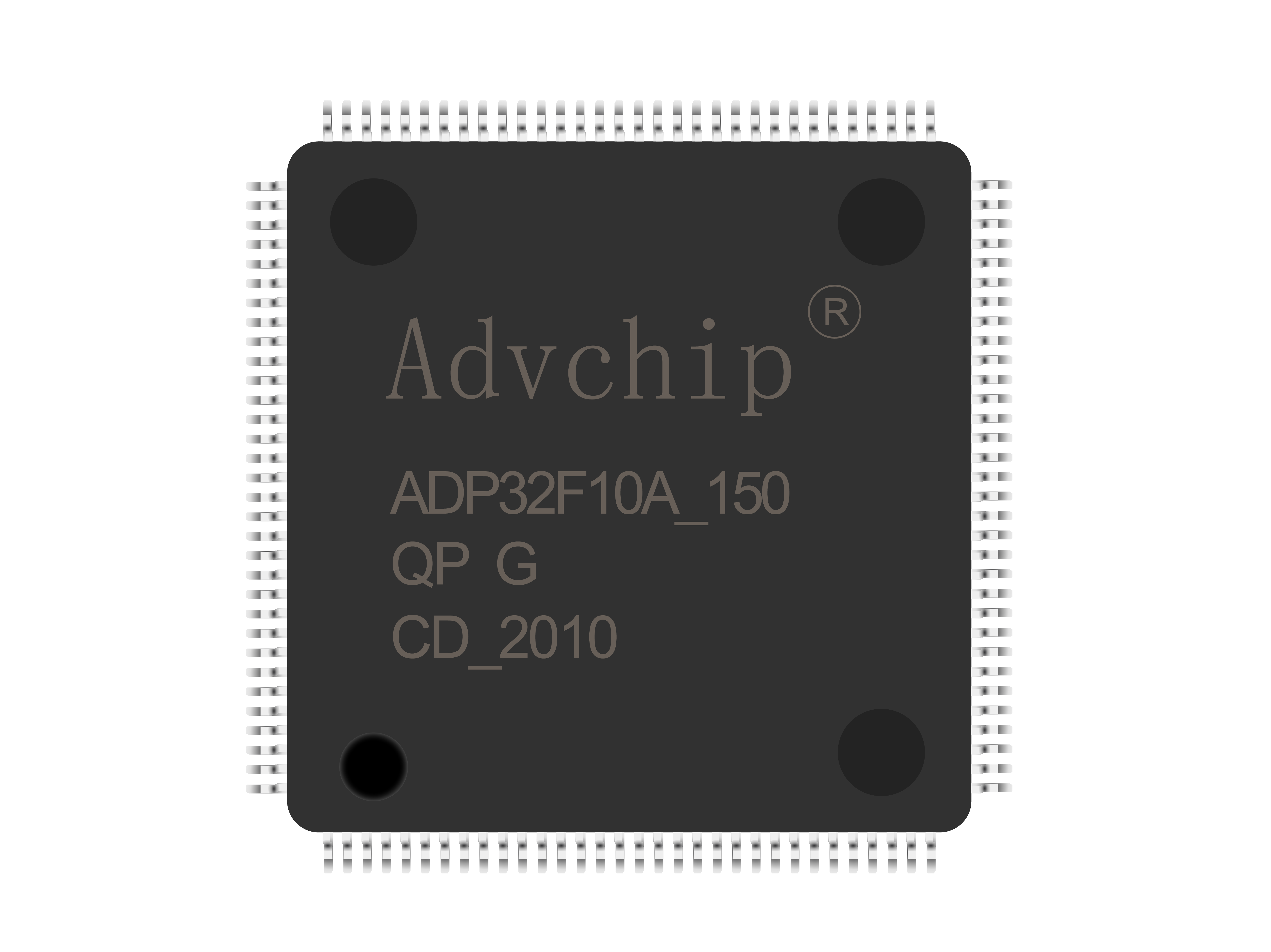
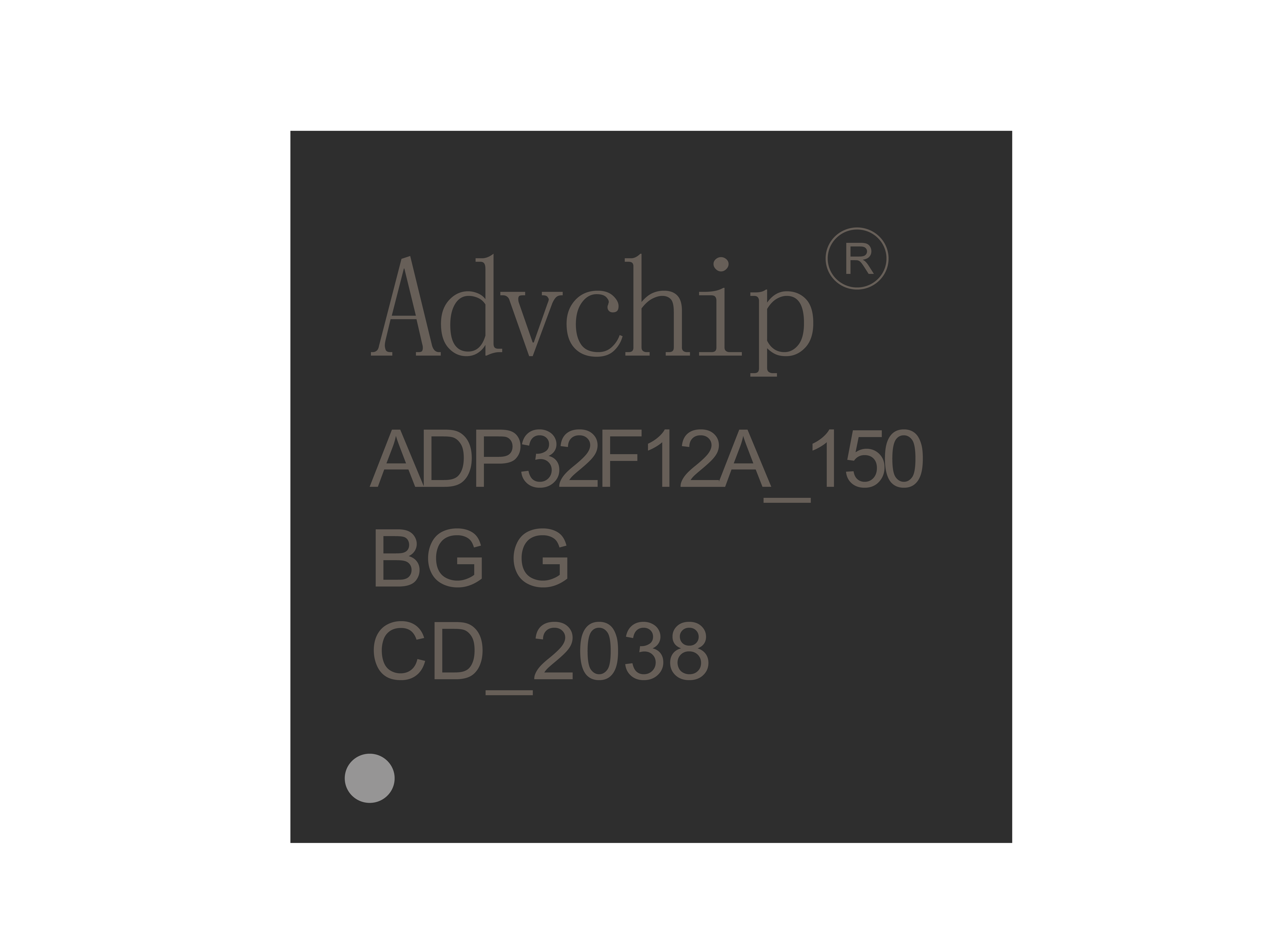
• Package Options
- BGA 179 (with external memory interface)
- LQFP176 (with external memory interface)
- LQFP128 (without external memory interface)
• Product Grade
- G: Industrial Grade
- G1: Industrial Grade Wide temperature range - C: Consumer grade


Co.,Ltd.")