Co.,Ltd.")
Co.,Ltd.")
 CN
CN
 EN
EN

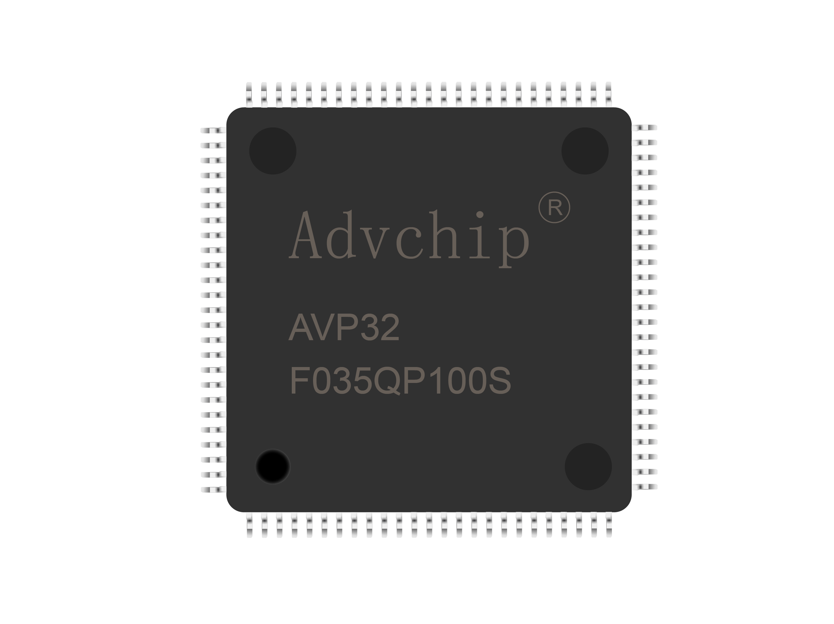
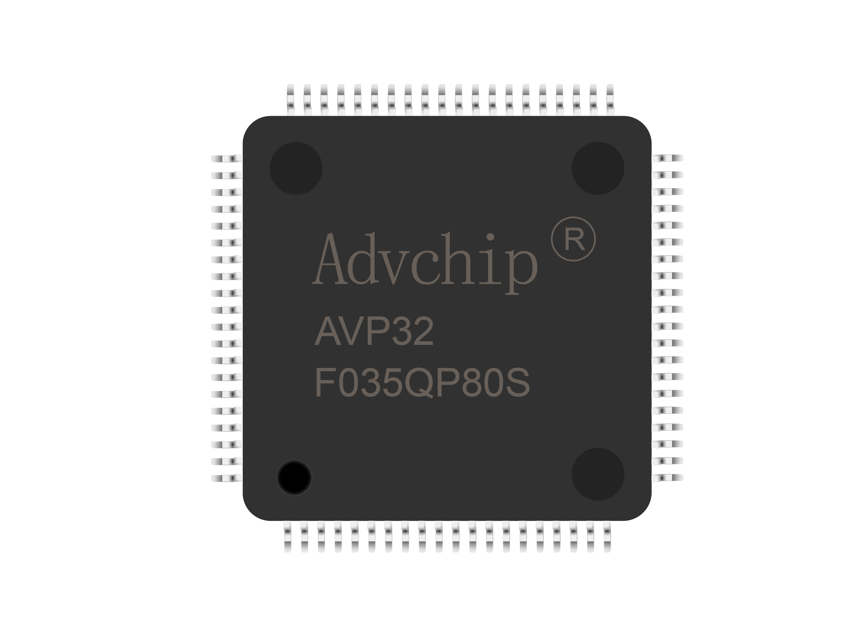
AVP32F035
AVP32F035 is a DSP controller based on a high-performance 32-bit AVP32 floating-point core, with a clock speed of up to 120MHz. It integrates a single precision floating-point arithmetic unit (FPU) and an independent programmable control loop accelerator (CLA), significantly enhancing real-time computing and parallel processing capabilities. It integrates a wide range of high-precision control peripherals, including up to 8 enhanced PWM modules (supporting HRPWM), 12 bit high-speed ADCs, and multiple communication interfaces. It adopts a 3.3V single power supply solution, integrates high-capacity memory and system protection functions, providing developers with a highly integrated solution. This processor is designed specifically for high-performance real-time control and is an ideal choice for driving industrial motor control, photovoltaic inverters, and digital power supplies.
Datasheet →industry
· High performance 32-bit floating-point processor core (AVP32)
- Main frequency 120MHz (single cycle 8.33ns)
- Supports 16 × 16 and 32 × 32 multiply accumulate (MAC) operations
- Supports 16 × 16 dual MAC operations
- Harvard bus architecture
- Linkage operations
- Fast interrupt response and processing
- Unified Memory programming model
- Efficient code (using C/C++and assembly language)
· Floating Point Unit (FPU)
- Supports native single precision floating-point operations
· Programmable Control Loop Accelerator (CLA)
-32 Bit Floating Point Mathematics Accelerator
- Code execution independent of the main CPU
· Viterbi, Complex Mathematics, CRC Unit (VCU)
- Supports complex multiplication, Viterbi operations, and cyclic redundancy check (CRC)
· Embedded Memory
- Supports up to 256KB of flash memory
Up to 100KB of random access memory (RAM)
-2KB of one-time programmable ROM (OTP)
· 6 Channel direct memory storage (DMA)
· Low device and system cost
-3.3V single power supply, no power timing requirements
- Integrated power on reset and undervoltage reset monitoring
- Low power operation mode
- No analog support pins
· Byte order: Small end byte order
Tag11
· Supports JTAG boundary scan
- IEEE Standard 1149.1-1990 Standard Test Access Port and Boundary Scan Architecture
· Clock
- Two internal zero pin oscillators
- On chip crystal oscillator/external clock input
- Watchdog timer module
- Lost clock detection circuit
· External Interrupt Extension (PIE) module
} Three 32-bit CPU timers
· } Advanced control peripherals
· 8 Enhanced Pulse Width Modulation (ePWM) modules
- a total of 16 PWM channels (supporting 8 HRPWM channels)
- independent 16 bit timers
· in each module 3 Input enhanced capture (eCAP) module
· 1 High Resolution Capture (HRCAP) modules
· Up to 2 Enhanced Orthogonal Encoder Pulses (eQEP) modules
· 12 Bit to digital converter (ADC) with dual sampling and holding (S/H) function
- up to 3.46MSPS
- up to 16 channels
· on-chip temperature sensor
· 128 Bit security key and lock
- Protect secure memory block
- Prevent firmware reverse engineering
· Serial port peripherals
-2 serial communication interface (SCI) modules
-2 serial peripheral interface (SPI) modules
-1 internal integrated circuit (I2C) bus
-1 multi-channel buffered serial port (McBSP) bus
16}
-1 Enhanced Controller Area Network (eCAN)
- Universal Serial Bus USB 2.0 specification
▪ Full speed device, full speed/low-speed host mode
· Up to 45 independent programmable, multiplexed general-purpose input/output (GPIO) pins with input filtering function
· high-level simulation features
- analysis and breakpoint function
- real-time debugging through hardware
· } Tag11 Package Options
-100 Pin QP Quad Flat Package (LQFP)
-80 Pin QP Quad Flat Package (LQFP)
· Temperature Options
- S: -40 ℃ to 105 ℃
Co.,Ltd.")