Co.,Ltd.")
Co.,Ltd.")
 CN
CN
 EN
EN

Product Overview
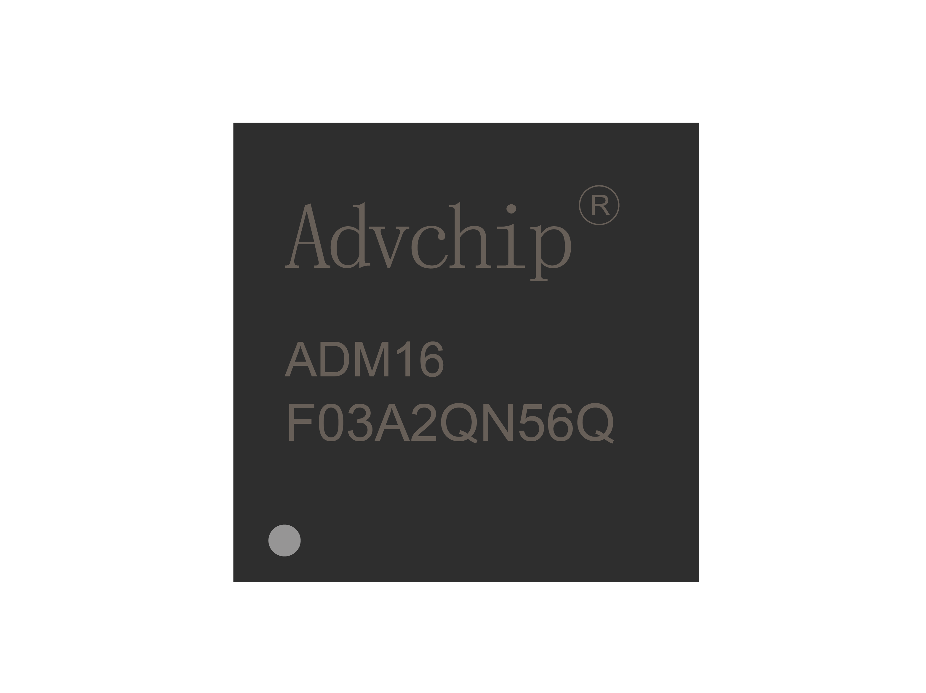
ADM16F03A2Q
ADM16F03A2Q is a high-performance SoC designed for automotive applications, with a clock frequency of up to 150MHz. It integrates an operational accelerator, operational amplifier, comparator, ADC, PWM controller, communication peripherals, pre driver, LDO, and LIN transceiver. It is directly powered by 12V and has high integration, making it convenient for networking; AEC-Q100 certification; Support multiple motor drives;
Datasheet →Automotive Standard
Product Features
● Single source power supply
-4.5V~40V
- Integrated LDO (pre drive 12V, core 1.2V, digital I/O 5V, analog 3V)
● Low power sleep mode current consumption
-20uA
● High performance 16 bit fixed-point DSP core
12}
-150MHz
- Harvard Bus Structure
- Fast Interrupt Response and Processing
● on-chip memory resources
-4K x 16 bit SARAM
- (256+256+32) x 16 bit DARAM
-32 K x 16 bits Flash
● operation acceleration unit
- division, square root
- arctangent
- Parker transform
-32-bit multiplication, addition, and shift
● 15 universal I/O+8 digits Input event manager EM1
-4 16 bit timer/counters
-8 PWM outputs (PWM1-6 are 3 sets of complementary outputs, PWM7/8 independent)
-1 set of orthogonal encoding units
-3 capture units (CAP1/2/3)
- configurable PWM cycle interrupt generation and ADC sampling trigger timing
● integrated three-phase high and low side half bridge drive circuit
- six NMOS Pre Driver
- gate drive circuit high side floating voltage reaches 200V
- Drive Capability IO+/IO -:+1.2A/2.0A VDRV=12V, VBS=12V
● ADC
-12 bits, conversion rate 1MSPS
-16 channels, with temperature sensor channels
- Channel Sorter, ADC can be set Sampling channel sequence
● Operational amplifier
-1 OP, can be used for bus current detection amplification
-3 PGAs, can be used for phase current detection amplification
● Voltage comparator
-3 voltage comparators, shared reference terminal, can be used for BEMF comparison detection
-2 voltage comparators, can form upper and lower limit value protection circuits The limit value can be configured through a pair of DAC connections to the comparator input
● Interrupts
-2 external interrupts
-29 peripheral interrupts set by PIE
● Digital delay filtering
-3 groups of independently configurable delay filtering units, corresponding to external interrupts, power protection, and CAP1/2/3
● Serial communication peripherals
- SPI (half duplex) SCI
● Clock
-10M on-chip oscillator
- PLL multiplication factor 1x~15x
● LIN transceiver
- compatible with "LIN2.x/ISO 17987-4:2016 (12V)/SAE J2602" standard
- with high-voltage LDO 5V voltage regulator output
} - Built in over temperature protection function (hot shutdown)
- Built in explicit timeout function
- Bus current limiting protection function
-5V voltage regulation and current limiting protection function
- Voltage regulator output undervoltage detection function
- Low power sleep mode
- Supports bus remote wake-up
- LIN data transmission rate can reach 20kbps
● Supports WDT
- Hardware based real-time debugging
● ESD level (HBM): 2000V
● Temperature range: -40 ° C~125 ° C (via AEC-Q100) ● Junction temperature: -40 ° C~150 ° C
Encapsulation Form
- QFN56 Encapsulation
-4.5V~40V
- Integrated LDO (pre drive 12V, core 1.2V, digital I/O 5V, analog 3V)
● Low power sleep mode current consumption
-20uA
● High performance 16 bit fixed-point DSP core
12}
-150MHz
- Harvard Bus Structure
- Fast Interrupt Response and Processing
● on-chip memory resources
-4K x 16 bit SARAM
- (256+256+32) x 16 bit DARAM
-32 K x 16 bits Flash
● operation acceleration unit
- division, square root
- arctangent
- Parker transform
-32-bit multiplication, addition, and shift
● 15 universal I/O+8 digits Input event manager EM1
-4 16 bit timer/counters
-8 PWM outputs (PWM1-6 are 3 sets of complementary outputs, PWM7/8 independent)
-1 set of orthogonal encoding units
-3 capture units (CAP1/2/3)
- configurable PWM cycle interrupt generation and ADC sampling trigger timing
● integrated three-phase high and low side half bridge drive circuit
- six NMOS Pre Driver
- gate drive circuit high side floating voltage reaches 200V
- Drive Capability IO+/IO -:+1.2A/2.0A VDRV=12V, VBS=12V
● ADC
-12 bits, conversion rate 1MSPS
-16 channels, with temperature sensor channels
- Channel Sorter, ADC can be set Sampling channel sequence
● Operational amplifier
-1 OP, can be used for bus current detection amplification
-3 PGAs, can be used for phase current detection amplification
● Voltage comparator
-3 voltage comparators, shared reference terminal, can be used for BEMF comparison detection
-2 voltage comparators, can form upper and lower limit value protection circuits The limit value can be configured through a pair of DAC connections to the comparator input
● Interrupts
-2 external interrupts
-29 peripheral interrupts set by PIE
● Digital delay filtering
-3 groups of independently configurable delay filtering units, corresponding to external interrupts, power protection, and CAP1/2/3
● Serial communication peripherals
- SPI (half duplex) SCI
● Clock
-10M on-chip oscillator
- PLL multiplication factor 1x~15x
● LIN transceiver
- compatible with "LIN2.x/ISO 17987-4:2016 (12V)/SAE J2602" standard
- with high-voltage LDO 5V voltage regulator output
} - Built in over temperature protection function (hot shutdown)
- Built in explicit timeout function
- Bus current limiting protection function
-5V voltage regulation and current limiting protection function
- Voltage regulator output undervoltage detection function
- Low power sleep mode
- Supports bus remote wake-up
- LIN data transmission rate can reach 20kbps
● Supports WDT
● Supports 4-wire fast program burning
● Supports JTAG online simulation
- Analysis and breakpoint functions- Hardware based real-time debugging
● ESD level (HBM): 2000V
● Temperature range: -40 ° C~125 ° C (via AEC-Q100) ● Junction temperature: -40 ° C~150 ° C
Encapsulation Form
- QFN56 Encapsulation

Co.,Ltd.")