Co.,Ltd.")
Co.,Ltd.")
 CN
CN
 EN
EN

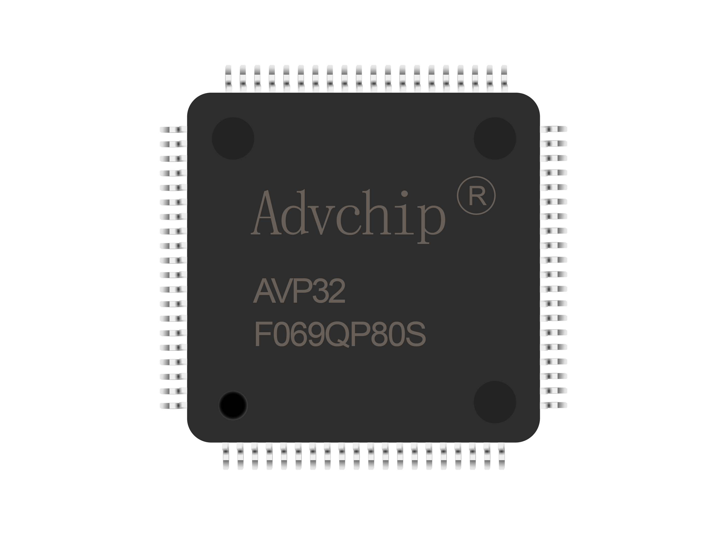
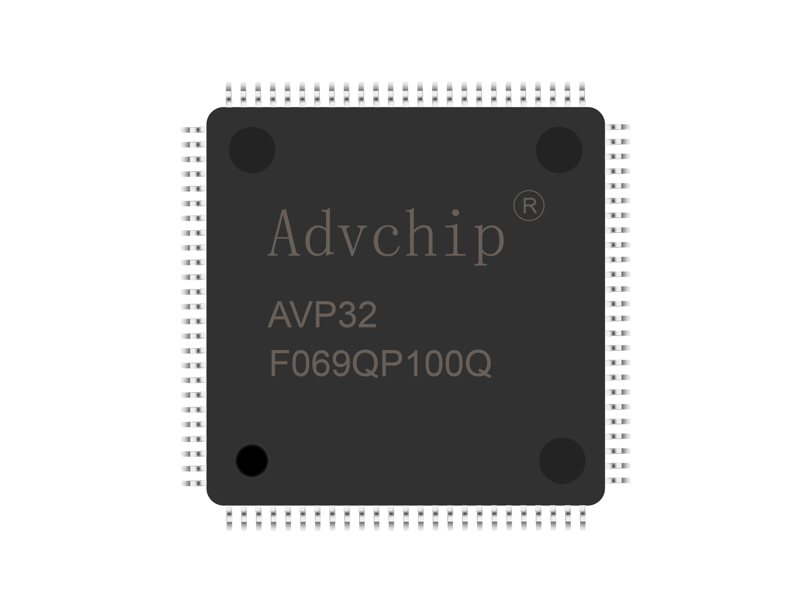
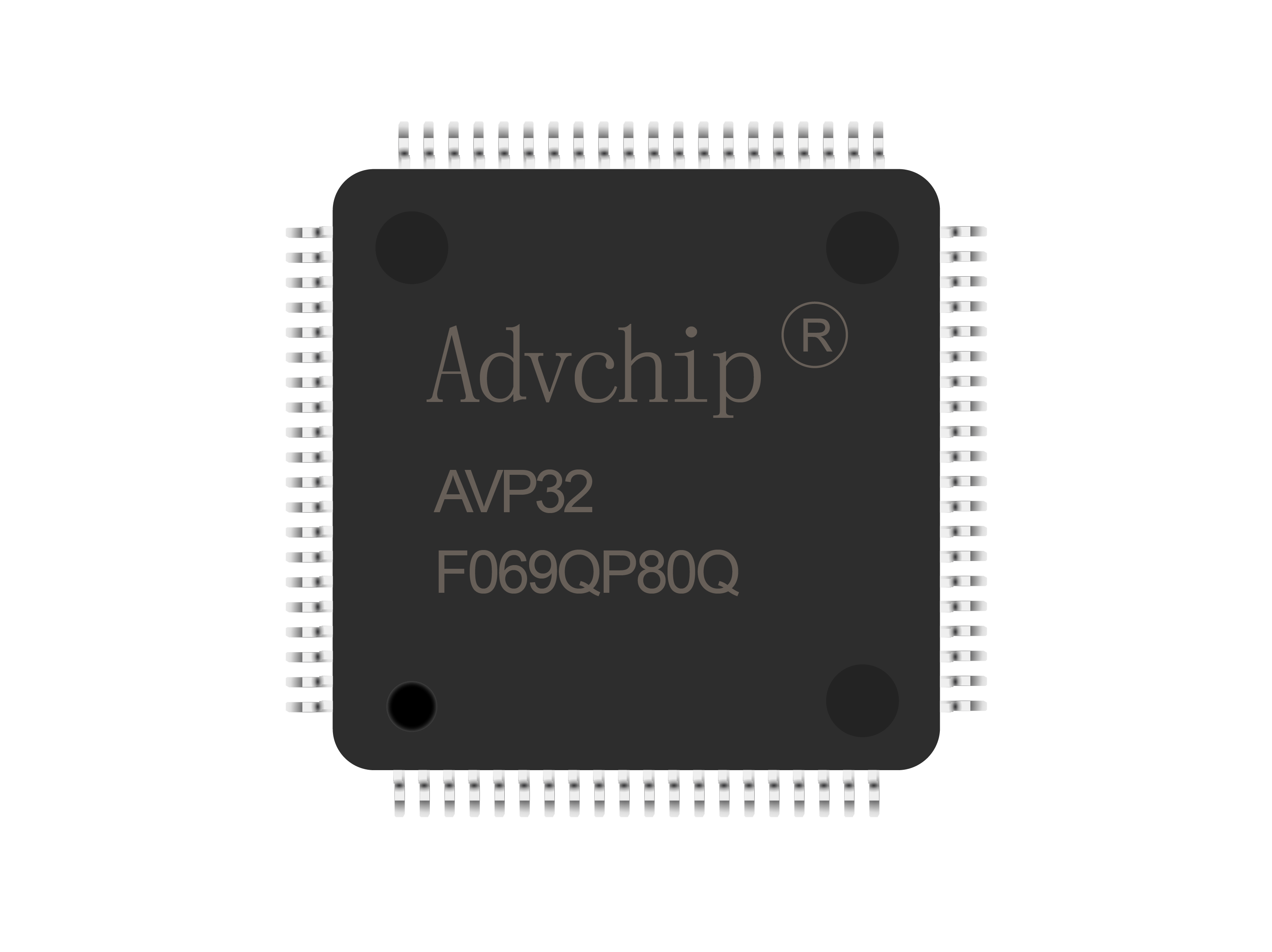
AVP32F069
AVP32F069 is a high-performance floating-point processor with a clock speed of up to 90MHz; The provided Control Loop Accelerator (CLA) can fully implement C programming and supports complex mathematical instructions and direct memory access, reducing CPU interrupt overhead. Multiple internal linear stabilized power supplies have achieved single power supply. Improvements have been made to the HRPWM module to provide dual edge control (frequency modulation). Provide up to 256KB Flash and 100KB RAM space; Multiple communication interfaces, including but not limited to USB. Mainly suitable for various applications in power electronics such as energy storage and photovoltaic inverters.
Datasheet →工业 车规
- Main frequency 90MHz (single cycle 11.11ns)
- Supports 16 × 16 and 32 × 32 multiply accumulate (MAC) operations
- Supports 16 × 16 dual MAC operations
- Supports single precision floating-point (FPU) operations
- Harvard Bus architecture
- Linkage operation
- Fast interrupt response and processing
- Unified storage programming model
- Code (using C/C++and assembly language)
● Programmable Control Loop Accelerator (CLA)
-32-bit Floating Point Mathematics Accelerator- Code execution independent of the main CPU
● Viterbi, Complex Mathematics, CRC Unit (VCU)
- Supports complex multiplication, Viterbi operations, and cyclic redundancy check (CRC)
● tag11 Embedded Memory
- Up to 256KB of Flash Memory
- Up to 100KB of Random Access Memory (RAM)
-2KB One Time Programmable (OTP) ROM
● 6 Channel Direct Memory Access (DMA)
● Low Device and System Costs
-3.3V Single Power Supply, No Power On Sorting
- Integrated Power On Reset and Undervoltage Reset Monitoring
- Low Power Operation Mode
- No Analog Support Pin
10} ● Byte order: Small end byte order
● Supports JTAG boundary scan
- IEEE Standard 1149.1-1990 Standard Test Access Port and Boundary Scan Describing Architecture
● Clock
}- Two internal zero pin oscillators
- on-chip crystal oscillator/external clock input
- watchdog timer module
- lost clock detection circuit
● Three external interrupt extension (PIE) modules
● } that can support all external interrupts. Bit CPU timer
● Advanced control peripherals
● 8 Enhanced Pulse Width Modulation (ePWM) Module
- A total of 16 PWM channels (supporting 8 HRPWMs)
- Independent 16 bit timers
● 3 Input enhanced capture (eCAP) modules
● Up to 4 high-resolution capture (HRCAP) modules
● Up to 2 enhanced orthogonal encoder pulse (eQEP) modules
● 12 Bit to digital converter (ADC) with dual sampling and holding (S/H) function
- up to 3.46MSPS
- up to 16 channels
● on-chip temperature sensor
● 128 Bit security key and lock
- Protect secure memory block
- Prevent firmware reverse engineering
●
- Two serial communication interface (SCI) modules
- Two serial peripheral interface (SPI) modules
- One internal integrated circuit (I2C) bus
- A Multi Channel Buffer Serial Port (McBSP) Bus
- An Enhanced Controller Area Network (eCAN)
- Universal Serial Bus USB 2.0 Specification
▷ Full Speed Device Mode
▷ Full speed/low-speed host mode
● Up to 54 independent programmable, multiplexed general-purpose input/output (GPIO) pins with input filtering function
● Simulation characteristics
- Analysis and breakpoint function
- Real time debugging through hardware
● Package options
-100 pin QP thin quad flat package (LQFP)
-80 pin QP thin quad flat package (LQFP)
● Temperature options
- S: -40 ° C to 125 ° C- S1: -55 ° C to 125 ° C (filtered)
- Q: -40 ° C to 125 ° C (certified by AEC-Q100)


Co.,Ltd.")