Co.,Ltd.")
Co.,Ltd.")
 CN
CN
 EN
EN

Jinxin launches automotive electronic water pump control solution based on ADM32F036A3Q
As a key executing component of the vehicle thermal management system, the electronic water pump is the core device for achieving vehicle thermal cycling and precise heat dissipation. The current mainstream solutions in the industry generally adopt a drive architecture based on BLDC (brushless DC) motors. Its ability to continuously and smoothly adjust motor speed, high-precision control performance, and comprehensive cost advantages have become important evaluation dimensions for the design and selection of solutions in this field. In response to the above market demand, Jinxin Electronics has launched an automotive electronic water pump solution based on ADM32F036A3Q DSP main control, suitable for 40-400W/12V power scenarios. This scheme adopts PWM/LIN communication and single resistor FOC control, which can significantly simplify system design and reduce costs while ensuring precise speed regulation and real-time fault diagnosis.
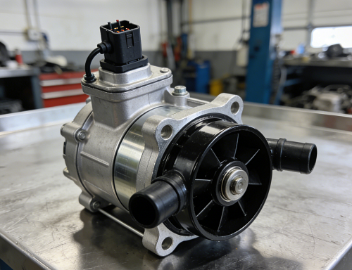
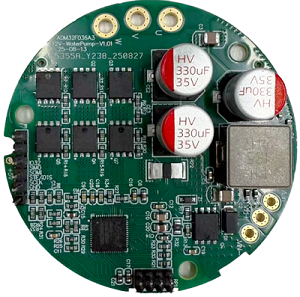
▲ Electronic water pump
ADM32F036A3Q Introduction to the main control chip
ADM32F036A3Q It is a 32-bit DSP vehicle grade improved version for motor control, integrating LDO, charge pump, and 6NMOS pre drive. It is equipped with a 100M main frequency 32-bit DSP processing core+CLA, enhanced control peripherals, CAN, CANFD, LIN (with transceiver), SPI, HRCAP modules, 12 bit ADC, voltage comparator, and temperature sensor; It can form a highly integrated motor control and drive core, directly driving power transistors to complete motor control, supporting multiple modes such as inductive, non inductive, square wave, and sine wave.
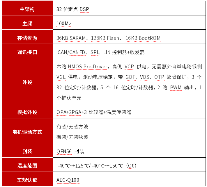
▲ ADM32F036A3Q motor control related resources
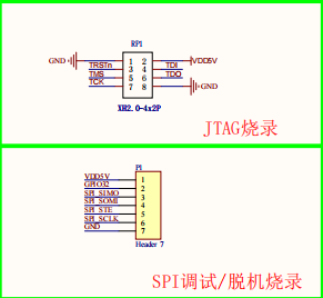
. At the same time, ADM32F036A3Q supports JTAG online simulation and supports fast burning mode with at least four wires for serial SCI mode.
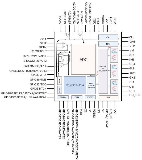
▲ Chip Pin Definition Layout
ADM32F036A3Q Application advantages
ADM32F036A3Q It is a highly integrated high-performance BLDC/PMSM controller, packaged as QFN56 and certified by AEC-Q100 automotive standards. Users can achieve excellent cost-effectiveness when designing motor control systems. ADM32F036A3Q integrates six NMOS Pre Drivers, charge pumps, and operational amplifiers internally, PGA, Comparator, high-speed ADC, CAN/CANFD, SCI, SPI, LIN controller+transceiver and other modules. At the same time, it adopts a high-performance 32-bit CPU with embedded 128KB Flash and a maximum operating frequency of 100MHz, which can meet the application requirements of high-performance brushless motor control and simplify the system hardware cost. Suitable for BLDC/PMSM motor square wave, SVPWM/SPWM, FOC drive control.
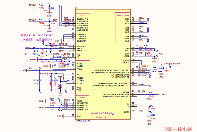
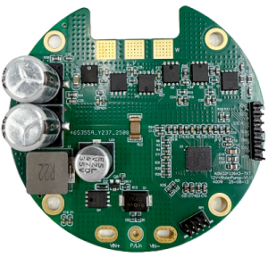
Hardware module introduction
Circuit module mainly includes: input anti reverse bus capacitor input part, ADM32F03A3Q minimum system, power bridge circuit, ADC bus sampling circuit, single resistor sampling operational amplifier sampling circuit, and PWM/LIN communication feedback circuit.
• Input anti reverse bus capacitor input part
Input is through N tubes to achieve anti reverse function. Use CE4, L1, and CE2 to form a π - type filter. Can effectively reduce power interference.
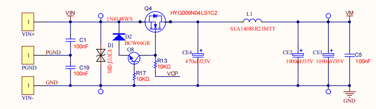
▲ Anti reverse Bus Circuit
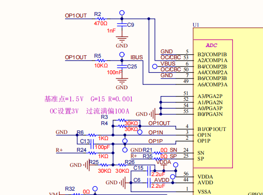
• ADM32F036A3Q Minimum System
ADM32F036A3Q The minimum system is shown in the following figure, including JTAG interface, SPI, LIN/PWM input, etc. The built-in operational amplifier OPA of the
system can be configured in differential mode through peripheral resistors for bus current sampling. The output result OP1OUT of the operational amplifier can be connected to COMP1 for hardware overcurrent protection. COMP1 can set different comparison levels internally, and once the threshold is triggered, the PWM signal can be directly locked.
When offline program burning is required, fast offline burning can be achieved by testing the pads with GPO19, GPO32, VDDIO, and GND signals using an in chip offline burning tool.
▲ Chip and Interface Schematic Diagram
• Power Bridge Circuit
The power bridge circuit adopts a configuration where both upper and lower transistors are NMOS,A total of 6 NMOS are used to form a three-phase H-bridge driving circuit.
A single sampling resistor of 0.001R is connected to the independent operational amplifier circuit of OP1 in ADM32F036A3Q through differential wiring, and the operational amplifier is input to the chip port for sampling and operation.
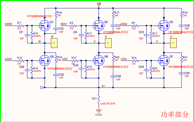
▲ Power Bridge Circuit Schematic
• ADC Bus Voltage Sampling Circuit
ADC The sampling bus sampling circuit divides the bus voltage value and sends it to the AD port of the chip to participate in the FOC operation.
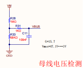
▲ ADC bus voltage sampling schematic
• Single resistor sampling op amp sampling circuit
uses an internal independent op amp OP1 group to perform differential op amp 15 times, which is sent to port A2 for overcurrent protection and to port A4 for constant power control.
▲ Operational amplifier circuit
• Charge pump circuit
The integrated charge pump does not require an external bootstrap circuit and can provide 100% duty cycle support.
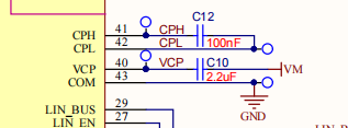
▲ Charge pump circuit part
• PWM/LIN communication feedback circuit
external input PWM/LIN signal, through the LIN transceiver module integrated inside the chip to achieve PWM/LIN communication feedback and remote sleep wake-up function through LIN_SUS and LIN-IN.
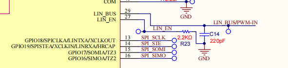
▲ PWM/LIN communication circuit
scheme description
adopts a single resistor sine wave, which is simple in circuit and low in cost. Sensorless FOC, power closed-loop, speed closed-loop. All protections are complete (overvoltage, overcurrent, locked rotor, phase loss, power) and other characteristics.
▲ 200 W ▲ 400W
Product Parameters
Voltage: DC12V
Power: 40-400W
Various protection features: VDS protection, GDF protection, overcurrent protection, short-circuit protection, overvoltage protection, undervoltage protection, stall protection, phase-absence protection, power protection, startup protection, and more.
This scheme uses the non inductive single resistor FOC algorithm, bus voltage ADC detection, and controls different speeds and fault feedback functions through PWM/LIN. It has the characteristics of strong carrying capacity, low noise, and stable waveform control.
Technical Support
Jinxin Electronics can provide customers with schematic diagrams, PCB reference board diagrams, source code, and corresponding software and hardware development technical support for the above solutions. For further information on the solution details, please call 0731-88731027.
Co.,Ltd.")