CN
CN
 EN
EN

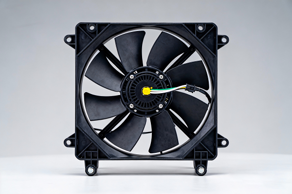
Jinxin Electronic Fan Sensorless FOC Drive Solution for Vehicle Thermal Management
With the evolution of automotive electrification architecture and the increasing demand for intelligent thermal management, electronic fans are transforming from traditional mechanical drives to high-precision, high response, and communicable motor drive systems. As a key executing component in vehicle thermal management, its control performance directly affects heat dissipation efficiency, system reliability, and vehicle energy consumption. Under this trend, integrated, low-noise, and intelligent diagnostic motor drive solutions have become a clear direction for industry development.
In response to the market demand for low-power brushless DC motor drives commonly used in car electronic fans, Jinxin Electronics has launched a 12V electronic fan overall solution suitable for the 400W-1000W power range. This scheme adopts PWM/LIN communication interface to achieve speed regulation and fault diagnosis feedback, supports sine wave drive architecture with single or dual resistor current sampling, has advanced noise suppression algorithm, adaptive start-up capability in both forward and reverse wind, and has comprehensive advantages such as simple circuit, stable control, and optimized system cost. The core control unit of the solution adopts the ADM32F036A3Q automotive grade digital signal processor (DSP) independently developed by Jinxin Electronics.
ADM32F036A3Q Introduction
ADM32F036A3Q is a 32-bit DSP vehicle grade improved version for motor control, integrating LDO, charge pump, and 6NMOS pre drive. It is equipped with a 100M main frequency 32-bit DSP processing core+CLA, enhanced control peripherals, CAN, CANFD, LIN (with transceiver), SPI, HRCAP modules, 12 bit ADC, voltage comparator, and temperature sensor; It can form a highly integrated motor control and drive core, directly driving power transistors to complete motor control, supporting multiple modes such as inductive, non inductive, square wave, and sine wave.
The following table is a brief introduction to the ADM32F036A3Q motor control resources:

▲ ADM32F036A3Q motor control related resources
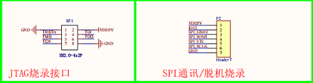
Meanwhile, ADM32F036A3Q supports JTAG online simulation and supports fast burning mode with a minimum of four wires for serial SCI mode. The following is the pin definition layout diagram of ADM32F036A3Q chip:
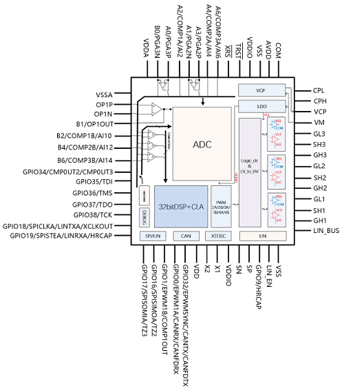
▲ Chip pin definition layout diagram
ADM32F036A3Q Application advantages
ADM32F036A3Q is a highly integrated high-performance BLDC/PMSM controller, packaged as QFN56 and certified to AEC-Q100 automotive standards. Users can achieve optimal cost-effectiveness when designing motor control systems. ADM32F036A3Q integrates six NMOS Pre Drivers, charge pumps, and operational amplifiers internally, PGA, Comparator, high-speed ADC, CAN/CANFD, SCI, SPI, LIN controller+transceiver and other modules. At the same time, it adopts a high-performance 32-bit CPU with embedded 128KB Flash and a maximum operating frequency of 100MHz, which can meet the application requirements of high-performance brushless motor control and simplify the system hardware cost. Suitable for BLDC/PMSM motor square wave, SVPWM/SPWM, FOC drive control.
Introduction to the Hardware Module
The main components of the circuit module include: input anti-inversion (with reserved high-side anti-inversion reference circuit) and filtering circuit, ADM32F036A3Q minimum system, power bridge circuit, ADC bus voltage sampling circuit, single-resistor sampling operational amplifier sampling circuit, and PWM/LIN communication feedback circuit.
• Input of the anti-countermeasures and filtering circuit section
The input is filtered through a N-channel tube to prevent reverse current (the gray section refers to a high-side anti-reverse circuit), and a Π-type filter circuit is added to reduce noise or interference signals.
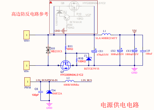
▲ Anti-bus circuit
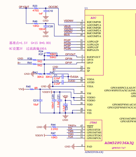
• The ADM32F036A3Q is a minimal system
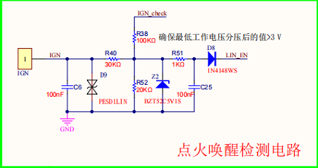
The ADM32F036A3Q's minimum system configuration, as shown in the figure below, includes a JTAG interface, SPI and LIN/PWM input ports, along with an ignition wake-up circuit module.
The system's built-in operational amplifier (OPA) can be configured in differential mode using external resistors for bus current sampling. Its output (OP1OUT) connects to COMP1 for hardware overcurrent protection. COMP1 allows setting different comparison thresholds, and once the threshold is exceeded, it immediately blocks the PWM signal.
For offline programming, the pins GPIO19, GPIO32, VDDIO, and GND are tested, and the chip's built-in offline programming tool enables rapid offline programming.
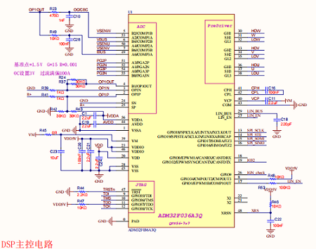
▲ Chip and interface schematic
• Power Bridge Circuit
The power bridge circuit employs NMOS transistors for both upper and lower stages, with six NMOS transistors forming a three-phase half-bridge driver circuit.
The single-sample resistor is 0.001Ω, and the differential trace leads to the independent operational amplifier circuit of OP1 in ADM32F036A3Q, where the input is sampled and processed through the chip port.
Using a single resistor sine wave, the circuit is simple and the cost is low. Sensorless FOC, power closed-loop, speed closed-loop. The characteristics include complete protection measures such as overvoltage, undervoltage, VDS, GDF, overcurrent, locked rotor, phase loss, and power.
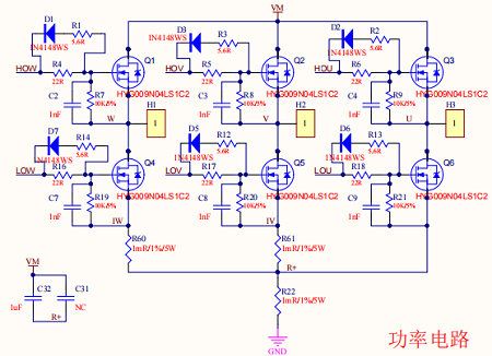
▲ Power bridge circuit schematic
• ADC bus voltage sampling circuit
The bus voltage sampling circuit delivers the voltage through a resistor divider to the chip's analog-digital (AD) port for processing.
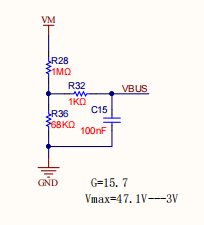
▲ Schematic diagram of AD bus voltage sampling principle
• Single-resistor sampling operational amplifier (op-amp) sampling circuit
The signal is amplified 15 times by the internal independent op-amp OP1, then fed into port A2 with overcurrent protection.
▲ Part of the operational amplifier circuit
• charge pump circuit
The integrated charge pump provides 100% duty cycle support without requiring an external bootstrap circuit.
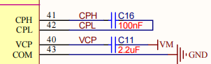
▲ The charge pump circuit section
• PWM/LIN communication feedback circuit
The system receives external PWM/LIN signals, processes them via the chip's integrated LIN transceiver module for PWM/LIN communication feedback, and executes remote sleep/wake functions through LIN Bus and LIN En.
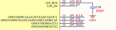
▲ PWM/LIN communication circuit
Solution Description
The circuit employs a single-resistor sine wave, featuring simplicity and low cost. It incorporates inductive FOC with closed-loop control for both power and speed. Comprehensive protection features include over/under-voltage, VDS, GDF, overcurrent, locked rotor, phase loss, and power protection.
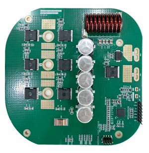
▲ 400W ▲ 1000 W
Product parameters
Motor speed: 2500
RPM Voltage: DC13.5V
Power: 400W/1000W
Multiple protection measures: VDS, GDF, overcurrent protection, short circuit protection, overvoltage protection, undervoltage protection, locked rotor protection, phase loss protection, power protection, start-up protection, etc.
This solution employs a contactless single-resistor FOC noise suppression algorithm, with bus voltage ADC detection and PWM/LIN control for variable speed operation and fault feedback. It features bidirectional startup capability, low noise levels, and stable waveform control.
Technical support
Jinxin Electronics provides clients with complete technical support for the aforementioned solutions, including schematic diagrams, PCB reference boards, source code, and corresponding software/hardware development. For further details, please contact us at 0731-88731027.