Overview
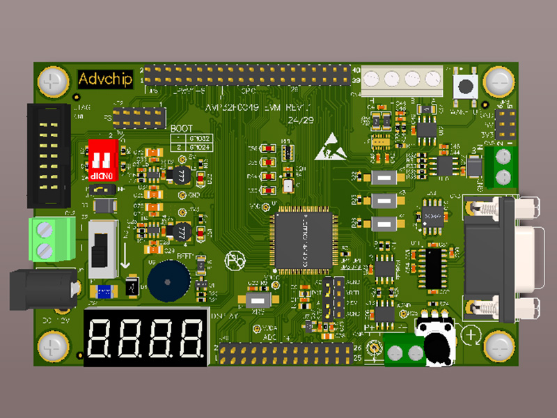
The AVP32F0049QP100S development board is a learning and secondary development platform based on the AVP32F0049QP100S chip. It can be directly embedded into users' product development process as a functional board, greatly reducing the development cycle. This development board is equipped with rich communication interfaces and a Hall current sensor that can be used to sample the output current ADC signal and amplify it through PGA signal. The CAN chip adopts a wake-up function and is connected to the DCDC enable pin. Users can control the wake-up and sleep of the development board power system through hardware wake-up of the on-board buttons or remote wake-up of CAN communication.
Performance Characteristics
Processor
● Main processor chip: AVP32F0049QP100S
● Floating point core, main frequency 100MHz, LQFP100 package
● On chip 128K x 16 bit Flash, 50K x 16 bit SRAM
● 21 high-precision 12 bit ADC inputs, 16 PWM outputs (including 16 HRPWM)
human-computer interaction
● 4-digit digital tube
● 4-channel LED lights
● 1-channel buzzer
● 3-channel independent buttons
External memory
● 1-channel RS232 (DB9) Connector)
● 1 RS485
● 1 CAN
● 1 LIN
● 1 FSI
Debugging
● All function IO port pin leads out
● JTAG emulator interface
● Main processor chip: AVP32F0049QP100S
● Floating point core, main frequency 100MHz, LQFP100 package
● On chip 128K x 16 bit Flash, 50K x 16 bit SRAM
● 21 high-precision 12 bit ADC inputs, 16 PWM outputs (including 16 HRPWM)
human-computer interaction
● 4-digit digital tube
● 4-channel LED lights
● 1-channel buzzer
● 3-channel independent buttons
External memory
● 2Kb EEPROM
● 32Mb Flash
External interface● 1-channel RS232 (DB9) Connector)
● 1 RS485
● 1 CAN
● 1 LIN
● 1 FSI
Debugging
● All function IO port pin leads out
● JTAG emulator interface


 CN
CN
 EN
EN


